We utilize One-Dimensional Photonic Crystals (1D PC) to sustain optical surface waves,
also known as Bloch Surface Waves (BSW) or Optical Tamm States. This technology offers significant advantages over traditional Surface Plasmon Resonance (SPR).
Unlike SPR (gold), our sensors use dielectric multilayers, providing narrower resonance peaks.
Narrower resonance peaks lead to higher sensitivity and lower detection limits.
The structure can be designed for any wavelength (UV to IR) and any polarization (TE or TM).
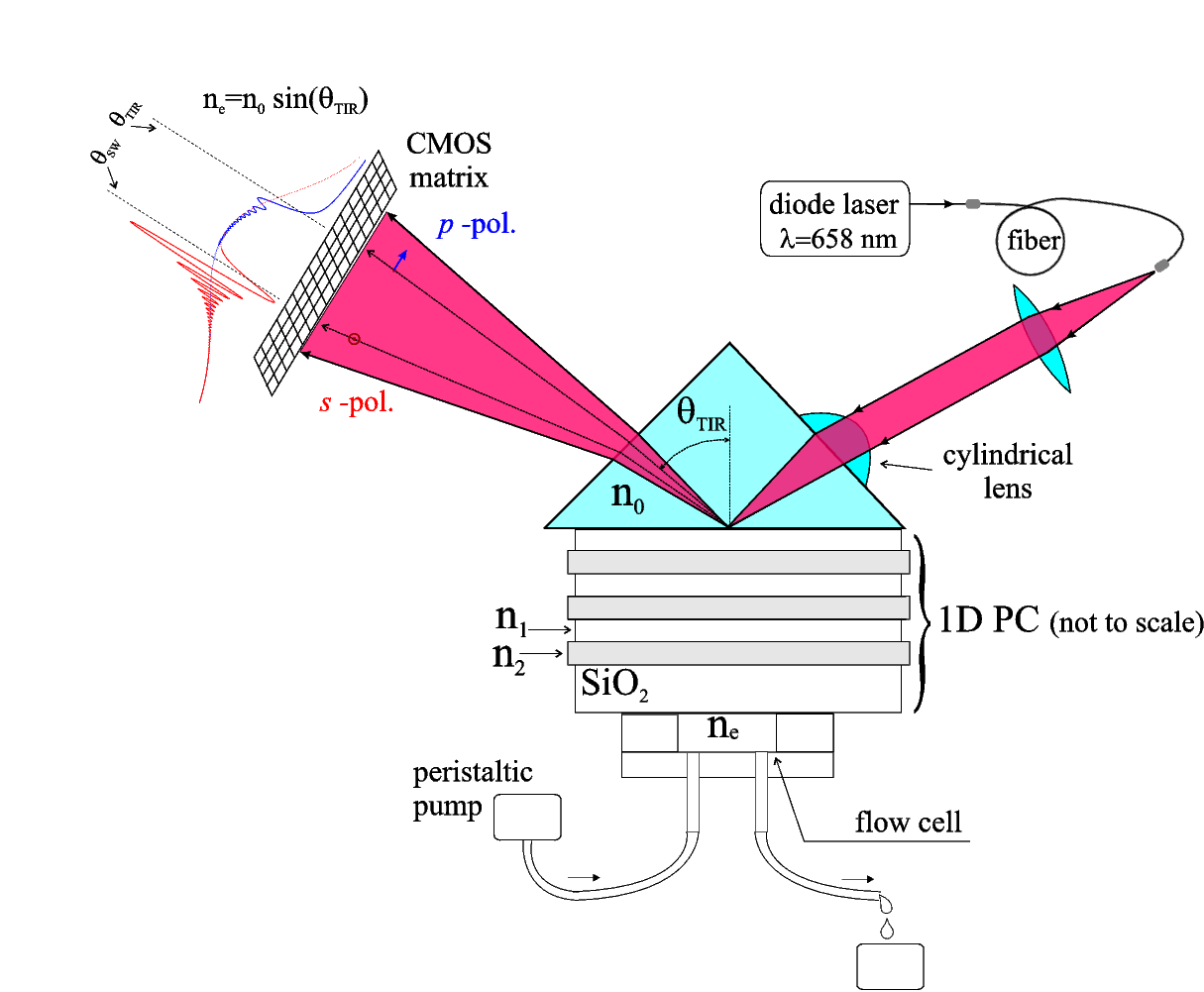
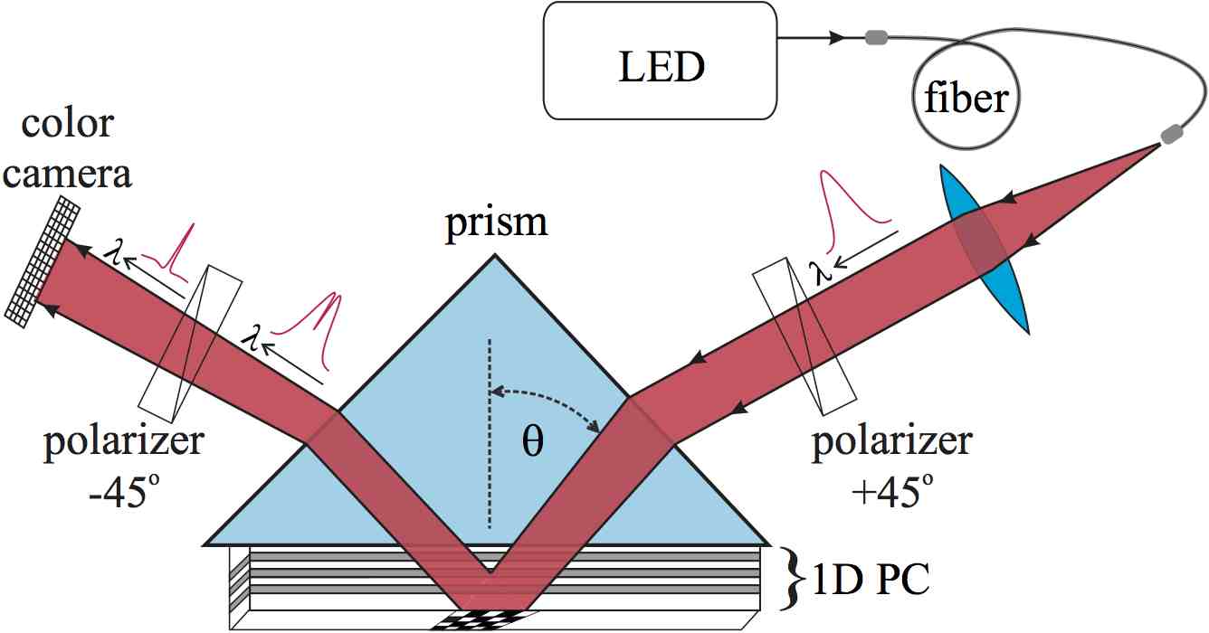
Figure 1: Sketch of the EVA 2.0 optical setup.
The EVA 2.0 uses a unique optical scheme that simultaneously registers:
This "RI-Referencing" allows the system to distinguish between actual binding kinetics and artifacts caused by temperature drifts or buffer exchanges, a common issue in standard biosensors.
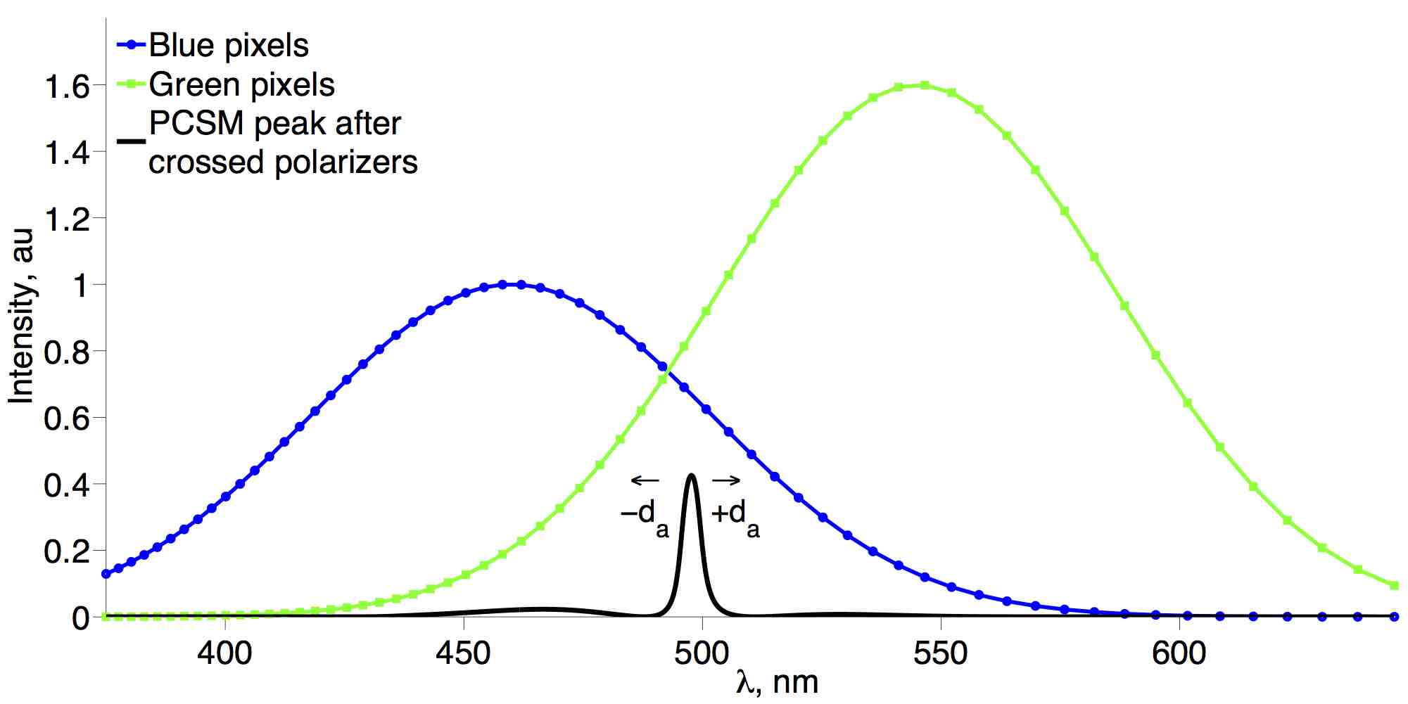
The EVA 3.0 utilizes a standard color CMOS camera to detect spectral shifts. The 1D PC chip is designed so that the resonance peak falls exactly between the Blue and Green pixel sensitivity maxima.
When binding occurs, the peak shifts, changing the ratio of intensities registered by the Blue and Green pixels. This allows for extremely precise wavelength determination without a spectrometer, enabling 2D imaging of the entire surface.